I've been doing some research on this device with a view to seeing how I can expand internal storage capacity because I need to occupy the sole USB port with my 4G LTE modem as that is my only source of internet in my home.
Let it be known that I have no knowledge of embedded Linux, Linux commands, Linux folder structures, config files etc. I've only ever worked on Windows and DOS so Linux itself is something new and strange to me, so please excuse me if I ask stupid questions or appear to get stuck on what may be considered basic things.
I do have a background in audio-visual equipment repair so working with PCBs, schematics, circuit diagrams, soldering and physical modifications I am pretty ok with.
PLEASE RIGHT CLICK ON IMAGES AND OPEN IN NEW TAB TO SEE THEM LARGER
THE NETGEAR WNDR3700v5 is produced for Netgear by a company called SerComm. Apart from perhaps the feature set and the plastic casing, it has almost nothing in common with earlier versions of the WNDR3700. This v5 is based around the Mediatek MT7621ST System On Chip.
A good point of reference for the technical specs is this page:
https://techinfodepot.shoutwiki.com/wik ... WNDR3700v5
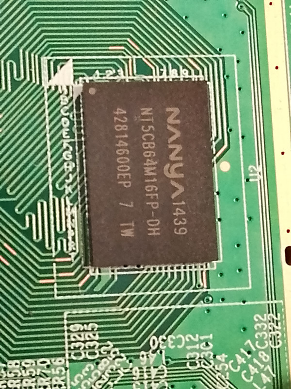
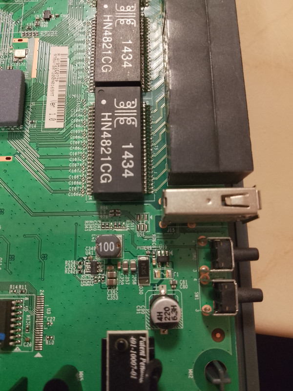
As far as I can see, this page appears to be accurate, except for where it claims the RAM chip to be a Nanya NT5CB64M16FP-DP. In my case it is a Nanya NT5CB64M16FP-DH as can be seen in this photo (The DP/DH may just be a typing error on that website as I can't seem to find reference of a DP existing):
This is inkeeping with other SerComm produced Netgear products that share the MediaTek_MT7621 - namely the Netgear R6220 router, the Netgear R6230 router, and the Netgear WAC104 Wireless Access Point. These products, and mine appear to share the same FCC ID according to the Netgear section of this table on the page:
https://techinfodepot.shoutwiki.com/wik ... Tek_MT7621
That makes me think they could all be based on the same PCB. What differs between mine and those other ones is that mine has only 16MB of NOR flash and the others have 128MB of NAND flash on board. The other difference you will notice is that while mine is advertised and sold by Netgear as a WiFi b/g/n device, the others add a/c connectivity. It is already a proven fact that installing Gargoyle (OpenWRT) on my device has in fact unlocked a/c functionality, so that brings me one step closer to the R6220 for example.
While the url https://techinfodepot.shoutwiki.com/wik ... WNDR3700v5 states that it has internal images of the WNDR3700v5, it actually has only a single image of the PCB of an R6220, which I will embed here:
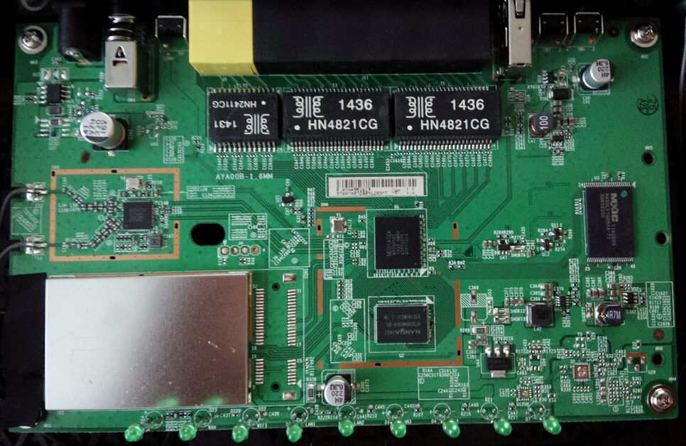
The NAND flash clearly visible at the right hand side of the photo.
Now to open my WNDR3700v5 and have a look inside.
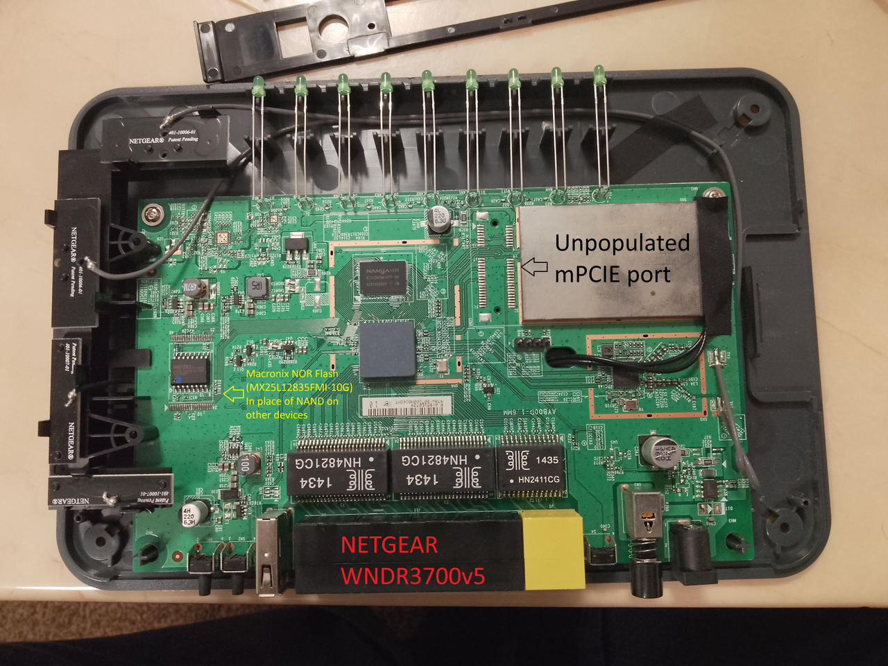
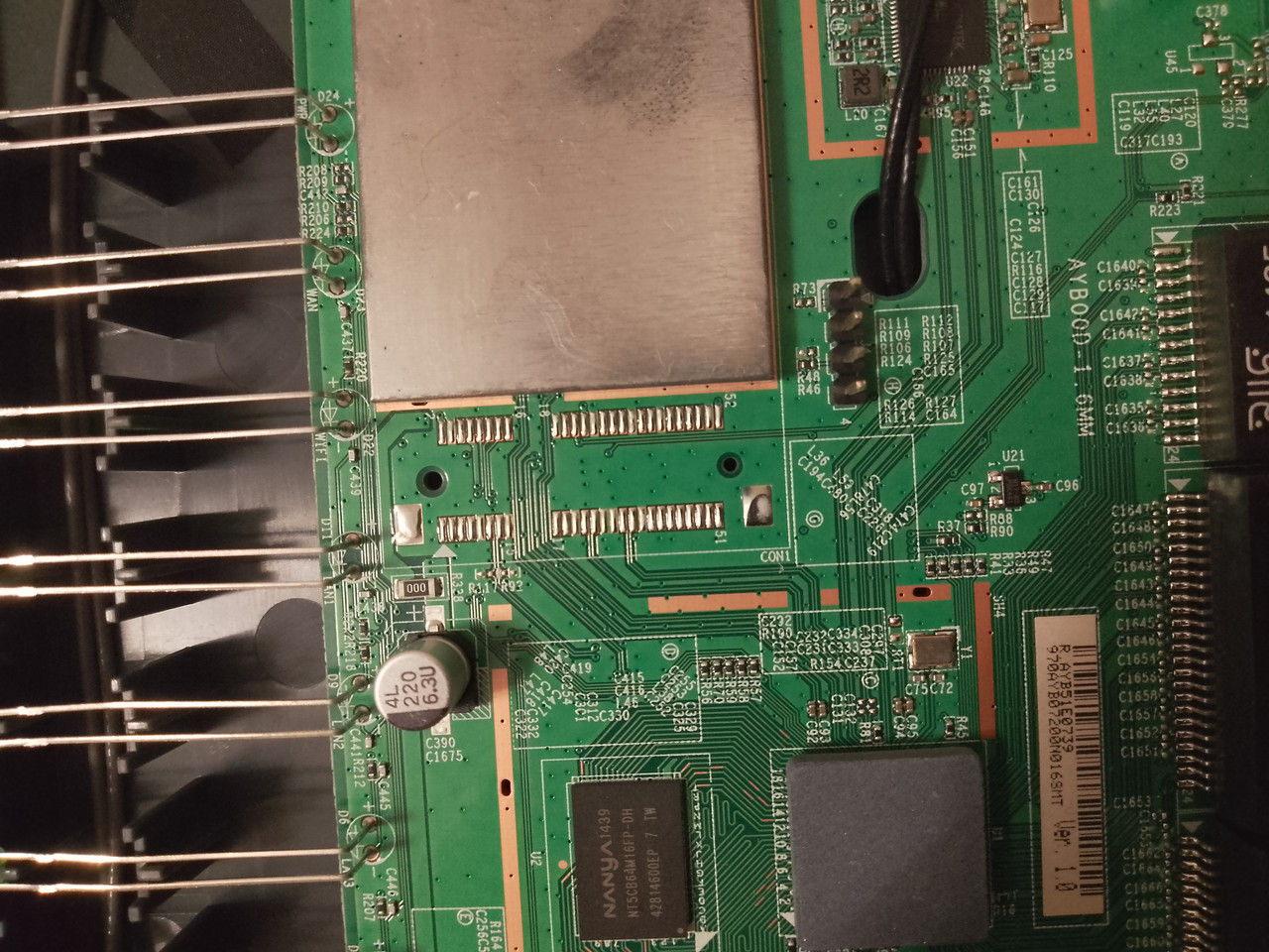
Very interesting. The NAND flash of the R6220 is indeed substituted for a Macronix MX25L12835FMI-10G NOR chip, BUT the solder pads for the NAND chip remain on the PCB. There are a few SMD capacitors and resistors (possibly 0 ohm resistors) around it, which can obviously not be there if a NAND chip were in place. Similarly there are R10 and C27 unpopulated which appear to be populated on the R6220.
Armed with this new found knowledge, 2 things are ringing in my head.
1 - Could it be as simple as removing the NOR chip, and replacing it with a larger capacity version of itself?
There appears to exist a MX25L25635FMI-10G https://www.digikey.co.uk/en/products/d ... 0G/4211590 which is double the capacity of the existing MX25L12835FMI-10G NOR chip. This would be a doddle to solder in due to the large legs with wide spacing, but the question remains, would I be able to flash the image onto a fresh chip of a different size?
2 - Could a NAND flash chip (as per the R6220) be put instead of the NOR chip and relevant SMD components moved? Without access to a circuit diagram or component list it would be difficult if not impossible to determine the values of those tiny components. Again the question remains. Would I be able to simply flash the same WNDR3700v5 image now that we have NAND in place of NOR, and the capacity is different OR would I be able to simply use the R6220 image instead?
I have the manufacturer's datasheet for the MediaTek MT7621ST System On Chip (complete pinout diagram included), and have learned that despite all of these Netgear routers only having a single USB port, the chipset actually supports 2 of them. It also supports SDXC card readers. A visual scan of the PCB revealed no unpopulated USB headers, so where were the pins of the second USB going? Were they even connected or simply ignored?
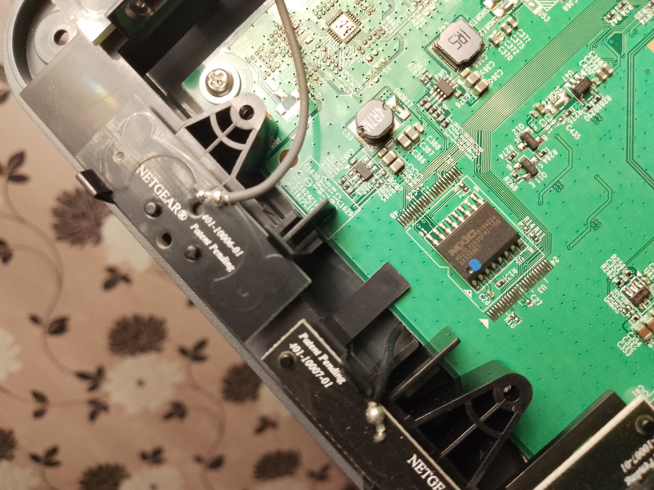
On quite a different note, the current DD-WRT image for the WNDR3700v5 is broken. Flashing that to my device caused it to get stuck in a boot loop. In order to help provide information that could help the developers at DD-WRT to fix their image I will try to get serial communication with my router. I found the 4 pin serial header on the PCB, but my attention also got drawn to something else.
In this photo you can see to the left of the serial header is an unpopulated mPCIe position on the PCB, which you may have spotted in an earlier image.
Searching around for "adding a USB port to MT7621ST", I came across this url:
https://www.eevblog.com/forum/projects/ ... 1608-zbt)/
Here the writer discovers that in his router (not a Netgear by the way) he was able to use the microPCIe connector with a USB adapter to gain an extra USB port. I shall embed his image here:
Does this open up another avenue of opportunity? More questions to be asked. Can I simply solder on a mPCIe socket and use a USB adapter as he did, or is there more to it than that? To further neaten it up could I even use a TF card adapter instead like this?

OR could I even use a micro PCI-E SSD which I happen to have a few spares of?

Due to it being the only router at home, I can't have it out of service for long. That's one of the reasons why the photos are so poor as I literally got up in the middle of the night and opened the router, took the photos and put it back before anyone knew.
The only other thing to tell you about is that there is another area of unpopulated solder pads on the board as well.
I don't really have any ideas at the moment of what this area of the board has been made for. I can see it is also unpopulated in the image of the R6220 PCB. It may be obvious to someone else what it is for. If you know, please comment.
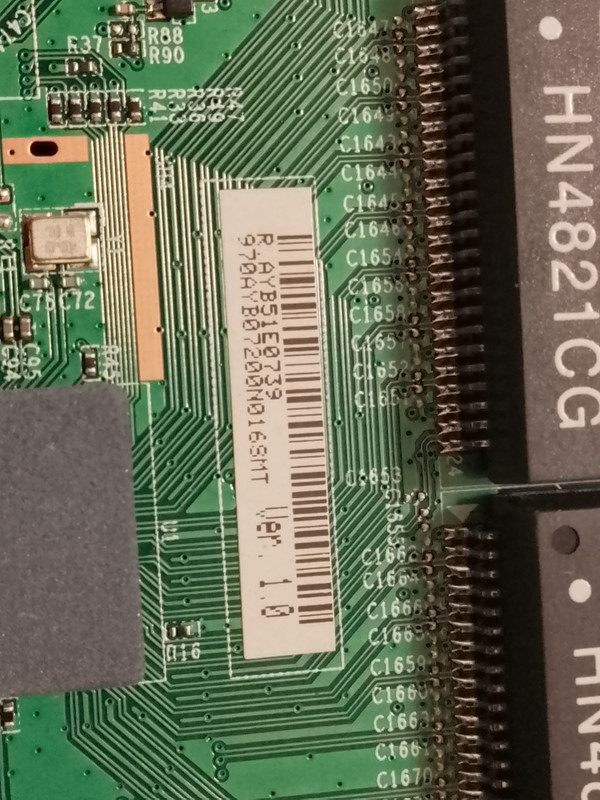
Finally here is a photo of the sticker on the PCB in case it is significant.
Please let me know your thoughts.